About Us
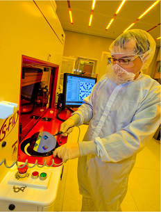
aBeam Technologies offers a variety of products to improve semiconductor manufacturing and nanofabrication. Our products are used to simulate and optimize nanolithography, metrology, maskmaking, and defect inspection. They are also used in the design and optimization of semiconductor equipment. In addition, the company sells e-beam pattern generators and provides top-level nanofabrication.
Our customers are top level semiconductor factories, equipment makers, as well as R&D labs and universities. aBeam Technologies has its headquarters in California, USA.
Semiconductor equipment is expensive. The chance to improve tool quality, enhance process quality, or extend its lifecycle for next generations makes our software a great return on investment. Details about our products and how they are implemented are listed in the Applications below; details about specific products are described in the Products area.
News and Events
There was a lot of changes in aBeam Technologies during the last few months. The major news are:
What used to be Nanofabrication and nano-Optics division at aBeam is now a separate company. The name of a new company is HighRI Optics. The main specialties of the company are:
- Development of novel high refractive index (RI) materials, including materials which are imprintable. The typical RI of materials is really high: from 1.7 to 2.05. Materials are organic, inorganic or hybrid, without use of nanoparticles. Some materials have patterning resolution down to 5 nm;
- Development and commercialization of revolutionary AFM probes for high resolution spectroscopic atomic force microscopy. The technology enables spectroscopic imaging with the resolution down to 30 nm or below, without big restrictions attributed to other methods. The probes are based on Campanile technology initially developed by Lawrence Berkeley National Laboratory;
- Nanofabrication and development of micro- and nano-optical elements. This includes optics nanoimprinted on the top of optical fibers.
The company continues collaboration with Lawrence Berkeley National Laboratory. The CEO of HighRI Optics is Dr. Keiko Munechika, who managed aBeam's Nanofabrication and nano-Optics division. For more information please refer to company's web-site www.highrioptics.com.
aBeam stopped selling a few software products: Chariot, aSEM, myCD, myTEM, Beametr, and qSEM.
Researchers at aBeam Technologies, in collaboration with Lawrence Berkeley National Laboratory and Argonne National Laboratory have developed a technology to fabricate test patterns with a minimum linewidth down to 1.5 nm. The designed patterns involve thousands of lines with precisely designed linewidths; these lines are combined in such a way that the distribution of linewidths appears to be random at any location. This pseudo-random test pattern allows nanometrological systems to be characterized over their entire dynamic range. For more details click here.
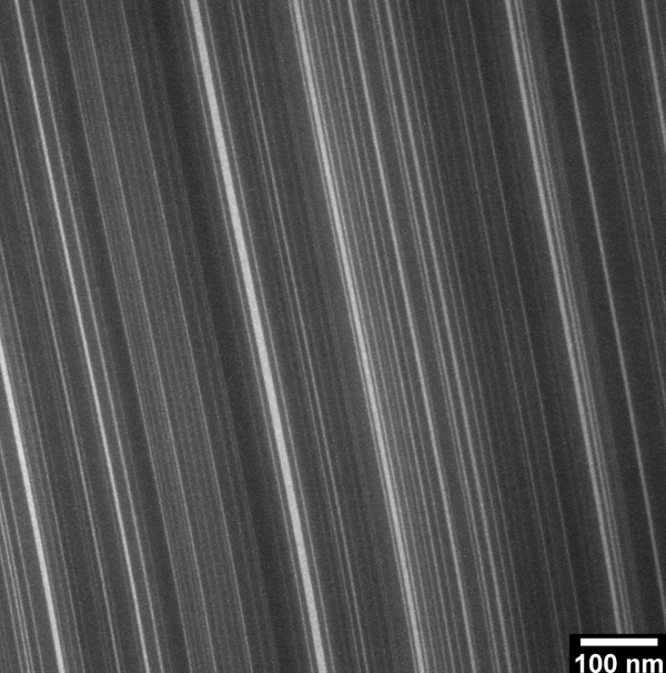
TEM image of fabricated test sample with minimum linewidths 1.5 nm
aBeam opens subsidiary in Japan
aBeam Technologies, Inc., announced a change in operations in Japan by establishing its subsidiary company, aBeam Technologies, Japan. The president of aBeam Technologies, Dr. Sergey Babin, said: "aBeam has established aBeam Technologies-Japan, Incorporated. The company will strengthen aBeam's ability to meet customers' demands and extend its business in Japan. The CEO of aBeam-Japan is Dr. Makoto Yoshimi, who has strong experience in the semiconductor industry on both the technical and business level. We believe that his deep expertise will benefit users of our products and increase the market for existing and future products."
aBeam Technologies develops software to simulate and optimize the fabrication processes in semiconductor manufacturing. Customers include chip-making factories, equipment makers, and maskshops. Read press release here.
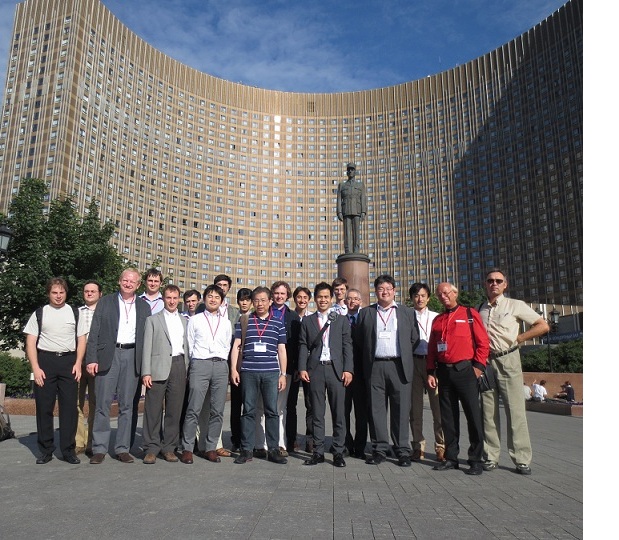
| Monte Carlo Workshop and User Meeting in Moscow, Russia | |
 |
August 2012, Newsletter:
|